(China (Mainland))

Product Summary
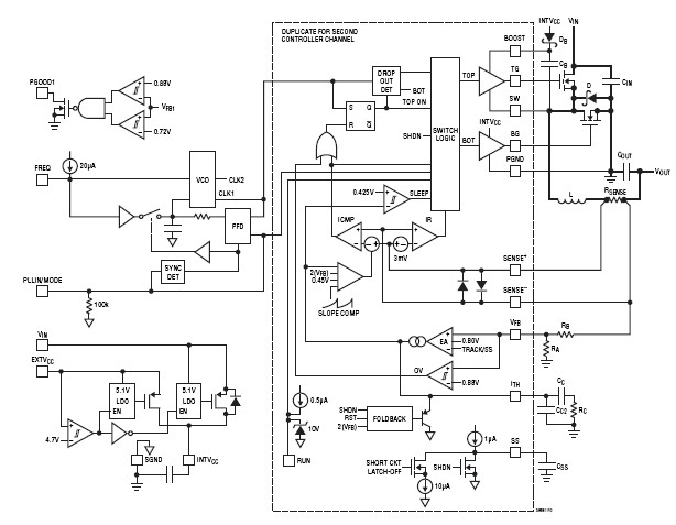
The LTC3858IGN-1#PBF is a Step-Down Controller. The LTC3858IGN-1#PBF is a high performance dual step-down switching regulator controller that drives all N-channel synchronous power MOSFET stages. A constant frequency current mode architecture allows a phase-lockable frequency of up to 850kHz. Power loss and noise due to the input capacitor ESR are minimized by operating the two controller outputs out of phase. The 170μA no-load quiescent current extends operating life in battery powered systems. OPTI-LOOP compensation allows the transient response to be optimized over a wide range of output capacitance and ESR values. The LTC3858IGN-1#PBF features a precision 0.8V reference and a power good output indicator. A wide 4V to 38V input supply range encompasses a wide range of intermediate bus voltages and battery chemistries. Independent soft-start pins for each controller ramp the output voltages during start-up. The output latch-off feature protects the circuit in short-circuit conditions. The applications of the LTC3858IGN-1#PBF include Automotive Systems, Battery Operated Digital Devices and Distributed DC Power Systems.
Parametrics
LTC3858IGN-1#PBF absolute maximum ratings: (1)Input Supply Voltage (VIN): –0.3V to 40V; (2)Topside Driver Voltages BOOST1, BOOST2: –0.3V to 46V; (3)Switch Voltage (SW1, SW2): –5V to 40V; (4)(BOOST1-SW1), (BOOST2-SW2): –0.3V to 6V; (5)RUN1, RUN2: –0.3V to 8V; (6)Maximum Current Sourced Into Pin from Source >8V: 100μA; (7)SENSE1+, SENSE2+, SENSE1– SENSE2– Voltages: –0.3V to 28V; (8)PLLIN/MODE, FREQ Voltages: –0.3V to INTVCC; (9)EXTVCC: –0.3V to 14V; (10)ITH1, ITH2,VFB1, VFB2 Voltages: –0.3V to 6V; (11)PGOOD1 Voltage: –0.3V to 6V; (12)SS1, SS2, INTVCC Voltages: –0.3V to 6V; (13)Operating Junction Temperature Range (Note 2): –40℃ to 125℃; (14)Maximum Junction Temperature (Note 3): 125℃; (15)Storage Temperature Range: –65℃ to 150℃; (16)Lead Temperature (Soldering, 10 sec) SSOP: 300℃.
Features
LTC3858IGN-1#PBF features: (1)Low Operating IQ: 170μA (One Channel On); (2)Wide Output Voltage Range: 0.8V≤VOUT≤24V; (3)Wide VIN Range: 4V to 38V; (4)RSENSE or DCR Current Sensing; (5)Out-of-Phase Controllers Reduce Required Input Capacitance and Power Supply Induced Noise; (6)OPTI-LOOPR Compensation Minimizes COUT; (7)Phase-Lockable Frequency (75kHz-850kHz); (8)Programmable Fixed Frequency (50kHz-900kHz); (9)Selectable Continuous, Pulse-Skipping or Burst ModeR Operation at Light Loads; (10)Very Low Dropout Operation: 99% Duty Cycle; (11)Adjustable Output Voltage Soft-Start; (12)Power Good Output Voltage Monitor; (13)Output Overvoltage Protection; (14)Output Latch-Off Protection During Short Circuit; (15)Low Shutdown IQ: 8μA; (16)Internal LDO Powers Gate Drive from VIN or EXTVCC; (17)No Current Foldback During Start-Up; (18)Tiny 4mm x 5mm QFN and Narrow SSOP Packages.
Diagrams
| Image | Part No | Mfg | Description |  |
Pricing (USD) |
Quantity | ||||||
|---|---|---|---|---|---|---|---|---|---|---|---|---|
 |
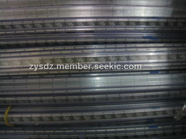
 LTC3858IGN-1#PBF |
|
IC REG CTRLR BUCK PWM CM 28-SSOP |
Data Sheet |
|
|
||||||
| Image | Part No | Mfg | Description | |
Pricing (USD) |
Quantity | ||||||
 |
LTC3025 |
Other |
|
Data Sheet |
Negotiable |
|
||||||
 |
LTC3025EDC#TR |
|
IC REG LDO ADJ .3A 6DFN |
Data Sheet |
|
|
||||||
|
LTC3025EDC#TRM |
|
IC REG LDO ADJ .3A 6DFN |
Data Sheet |
|
|
||||||
|
LTC3025EDC#TRMPBF |
|
IC REG LDO ADJ .3A 6DFN |
Data Sheet |
|
|
||||||
|
LTC3025EDC#TRPBF |
|
IC REG LDO ADJ .3A 6DFN |
Data Sheet |
|
|
||||||
|
LTC3025EDC-1#TRMPBF |
|
IC REG LDO ADJ .5A 6DFN |
Data Sheet |
|
|
||||||